
Before you start
- Board and software
- Classic ESP32-WROOM-32/32E DevKit with the listed GPIOs exposed and unused. Arduino IDE 2.x; esp32 by Espressif Systems 3.3.2 (review baseline, not a latest-release claim). Select the documented board or ESP32 Dev Module for a generic WROOM board. Other families need their own pin map. Serial Monitor: 115200 baud.
- Supported hardware
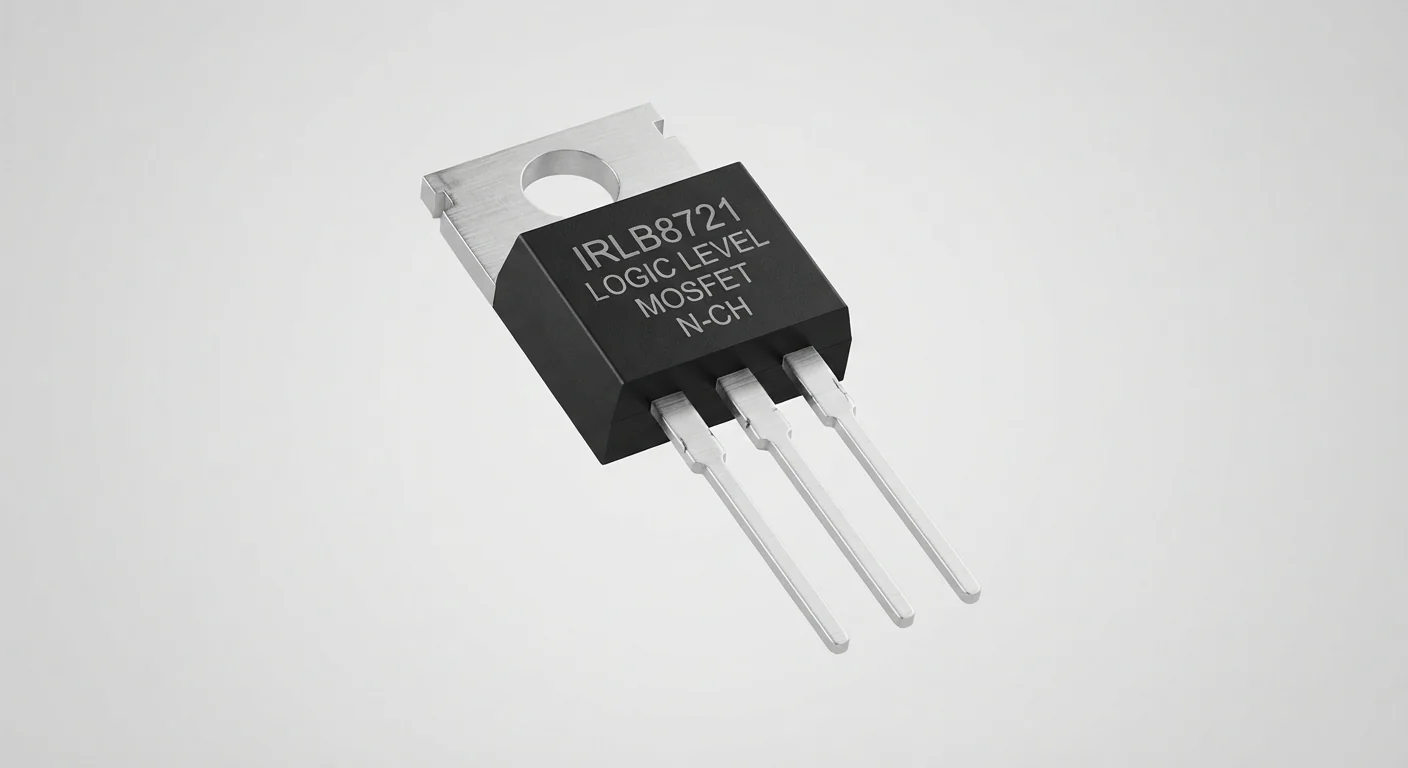
- Documented Infineon IRLB8721PbF TO-220AB, plus TI SN74AHCT125N DIP-14 buffer. Confirm gate/drain/source using the manufacturer package drawing; the metal tab is drain. Illustration markings do not authenticate a device.
- Prerequisites and parts
- Complete Blink and resistor identification. MOSFET, SN74AHCT125N, 100 nF bypass capacitor, 10 kOhm buffer-input pull-down, 100 kOhm gate-source pull-down, 1 kOhm gate resistor, red LED and 1 kOhm LED resistor. External regulated 5 V supply; ESP32 via USB, positive rails separate.
- Libraries
- No extra library. Arduino-ESP32 3.3.2 GPIO and millis APIs.
- Expected result
- The external LED is ON for 500 ms and OFF for 1000 ms; GPIO drives only the buffer input.
- Verification status
- Documentation and source review only. Not compiled or tested on hardware. The approved product-style illustration identifies a family, not a verified physical pin layout or manufacturer-authenticated board. Follow the logical diagram and documentation for your actual part.
Overview
A MOSFET’s gate voltage controls the path from drain to source. Unlike an NPN base, it mainly draws current while its gate capacitance charges or discharges. This circuit switches the ground side of a small LED load.
IRLB8721 is often advertised as logic-level, but its guaranteed on-resistance is specified at 4.5 V and 10 V gate drive. The threshold value describes a tiny test current, not full-load conduction. A 5 V AHCT buffer accepts ESP32’s 3.3 V command and gives this slow demonstration a defined higher gate drive.
Technical Specifications
Arduino library: Arduino-ESP32 3.3.2 (no additional library)
| Specification | Value | Why it matters |
|---|---|---|
| Guaranteed RDS(on) test points | 4.5 V and 10 V gate drive | No guaranteed 3.3 V on-resistance claimed. |
| Reference terminals | Gate, drain, source; tab = drain | Use the exact TO-220AB package drawing. |
| Example load | One red LED and 1 kOhm resistor | A few mA design estimate; no heatsink/current claim inferred from package ratings. |
Pinout
- 74AHCT125 pin14 VCC Supply External regulated +5 V Use SN74AHCT125N DIP-14; not an HC125.
- 74AHCT125 pin7 GND Return Common GND ESP32 GND and external supply negative.
- 74AHCT125 pin2 1A Input GPIO25 + 10 kOhm to GND Pull-down holds input LOW during reset.
- 74AHCT125 pin1 /1OE Enable GND Active LOW; channel1 enabled.
- Unused /OE: 4,10,13 Disable +5 V Outputs6,8,11 left unconnected.
- Unused A: 5,9,12 Input GND Do not leave CMOS inputs floating.
- 100 nF ceramic Bypass Between pins14 and7 Close to buffer; no polarity.
- 74AHCT125 pin3 1Y Gate drive 1 kOhm → MOSFET gate No connection back to GPIO.
- 100 kOhm resistor Pull-down MOSFET gate to source Keeps gate discharged when buffer is unavailable.
- IRLB8721 source Return Common GND Confirm manufacturer package view.
- External +5 V Load supply 1 kOhm → red LED anode Separate LED current-limiting resistor.
- Red LED cathode Switched load IRLB8721 drain Tab is also drain; avoid accidental shorts.
Wiring Diagram
GPIO25 → AHCT 1A; 1Y → 1 kOhm → gate; source → common GND. +5 V → 1 kOhm → LED → drain. Buffer5 V, enables/unused inputs, bypass and pull-downs as listed.
| Component terminal | ESP32 / circuit connection | Purpose and qualification |
|---|---|---|
| 74AHCT125 pin14 VCC | External regulated +5 V | Use SN74AHCT125N DIP-14; not an HC125. |
| 74AHCT125 pin7 GND | Common GND | ESP32 GND and external supply negative. |
| 74AHCT125 pin2 1A | GPIO25 + 10 kOhm to GND | Pull-down holds input LOW during reset. |
| 74AHCT125 pin1 /1OE | GND | Active LOW; channel1 enabled. |
| Unused /OE: 4,10,13 | +5 V | Outputs6,8,11 left unconnected. |
| Unused A: 5,9,12 | GND | Do not leave CMOS inputs floating. |
| 100 nF ceramic | Between pins14 and7 | Close to buffer; no polarity. |
| 74AHCT125 pin3 1Y | 1 kOhm → MOSFET gate | No connection back to GPIO. |
| 100 kOhm resistor | MOSFET gate to source | Keeps gate discharged when buffer is unavailable. |
| IRLB8721 source | Common GND | Confirm manufacturer package view. |
| External +5 V | 1 kOhm → red LED anode | Separate LED current-limiting resistor. |
| Red LED cathode | IRLB8721 drain | Tab is also drain; avoid accidental shorts. |
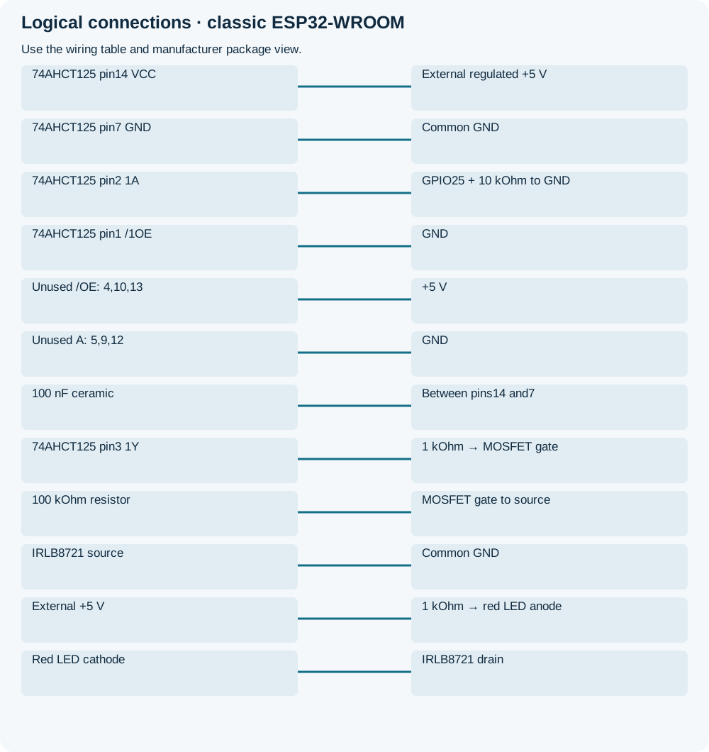
Open wiring diagram at full size (new tab)
-
1
Unplug USB and external supply. Match the MOSFET package and DIP-14 buffer pin drawings.
-
2
Wire every buffer supply/enable/unused input and pull-down, then the LED load. Join grounds; do not join external +5 V to the USB-powered board.
-
3
Upload and apply regulated 5 V. Compare LED switching with Serial commands.
Wiring and matching Arduino code
Slow buffered MOSFET switch
GPIO25 → AHCT 1A; 1Y → 1 kOhm → gate; source → common GND. +5 V → 1 kOhm → LED → drain. Buffer5 V, enables/unused inputs, bypass and pull-downs as listed.
irlb8721_mosfet.ino
#include <Arduino.h>
constexpr uint8_t OUTPUT_PIN = 25;
bool active = false;
uint32_t changedAt = 0;
void setup() {
  Serial.begin(115200);
  pinMode(OUTPUT_PIN, OUTPUT);
  digitalWrite(OUTPUT_PIN, LOW);
  Serial.println("Starts OFF; repeating on/off demonstration");
}
void loop() {
  const uint32_t now = millis();
  const uint32_t interval = active ? 500 : 1000;
  if (now - changedAt >= interval) {
    changedAt = now;
    active = !active;
    digitalWrite(OUTPUT_PIN, active ? HIGH : LOW);
    Serial.println(active ? "ON" : "OFF");
  }
}
Do not connect GPIO directly to the gate in this reference circuit. This sketch uses ordinary HIGH/LOW, not obsolete LEDC channel APIs. It is not a high-frequency PWM gate-driver design.
Expected Output
The LED should follow the repeated ON/OFF commands. Serial is a command log, not evidence of gate voltage or successful switching. If the LED stays on, inspect source/drain orientation and wiring before trying a larger load.
How it works
With /1OE grounded, the AHCT channel passes the command without inversion. Its 5 V output raises gate voltage relative to the grounded source. The series gate resistor limits transient charging current; the pull-down discharges the gate when drive is absent. Larger or faster loads need gate-charge, switching-loss, safe-operating-area, thermal and supply analysis. Motors/coils also need an appropriate flyback path; the MOSFET body diode is not a substitute for a diode across a low-side inductive load.
Troubleshooting
| Problem | Possible cause | Solution |
|---|---|---|
| Always on | Reversed source/drain, floating gate or load bypassing drain. | Power off; trace the manufacturer terminals and both pull-downs. |
| Never on | Disabled buffer, wrong chip family or missing common ground. | Verify AHCT markings, 5 V supply, /1OE and named signal paths. |
| Hot transistor | Insufficient drive, excessive load or fast switching losses. | Disconnect. Do not extrapolate from package current ratings; return to the small LED reference. |
Where you use it
- Learning buffered gate drive
- Small resistive/LED load switching
- Preparation for a separately engineered low-voltage power stage
Continue learning
FAQ
Not for every part/load. This datasheet does not guarantee low on-resistance at 3.3 V; the reference uses a buffer.
Do not assume it. This example relies on AHCT TTL-compatible inputs while powered at 5 V.
Technical references
- Infineon IRLB8721 datasheet — Gate-drive test points, threshold and package.
- TI SN74AHCT125 datasheet — 5 V operation, TTL inputs, DIP pin map and enables.
- Arduino-ESP32 3.3.2 — GPIO/timing review baseline.
- Arduino-ESP32 3.3.2 GPIO implementation — Initialize the GPIO bus with pinMode before digitalWrite; hardware pull-down provides reset bias.